LM22FD-B
22 nm FD-SOI, body-bias tunable
Standard-cell libraries complete and checked; timing characterization next.
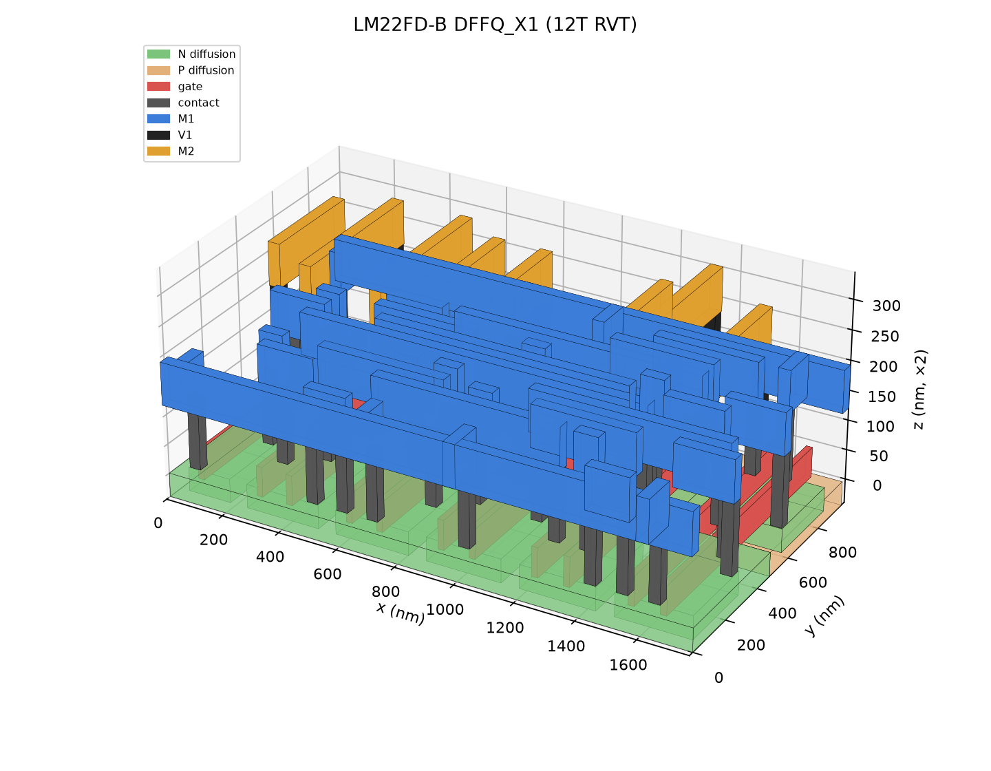
LM22FD-B is a 22 nm-class fully depleted silicon-on-insulator (FD-SOI) kit. The transistor channel is a 6 nm silicon film on a 20 nm buried oxide, so the well underneath acts as a second gate. Biasing that back gate moves the threshold voltage by about 75 mV per volt, which makes speed and leakage adjustable after manufacturing. That knob is the heart of this kit.
Why FD-SOI at 22 nm
FD-SOI is the low-power, low-voltage alternative to FinFET: a planar process with excellent electrostatics, low variability and the unique ability to trade speed for leakage at run time. It is used for IoT, automotive radar, edge AI and wireless chips, where energy matters more than peak speed.
Technology at a glance
| Supply | 0.8 V nominal |
| Contacted gate pitch | 104 nm |
| Gate length | 20 nm |
| Silicon film / buried oxide | 6 nm / 20 nm |
| Back-gate coupling | about 75 mV of threshold per volt of bias |
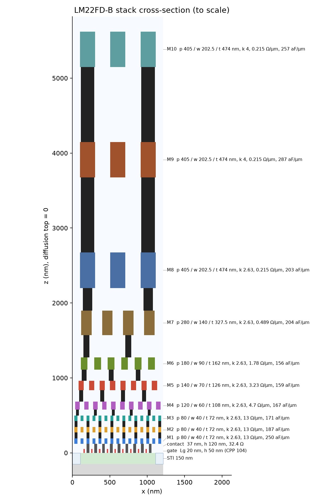
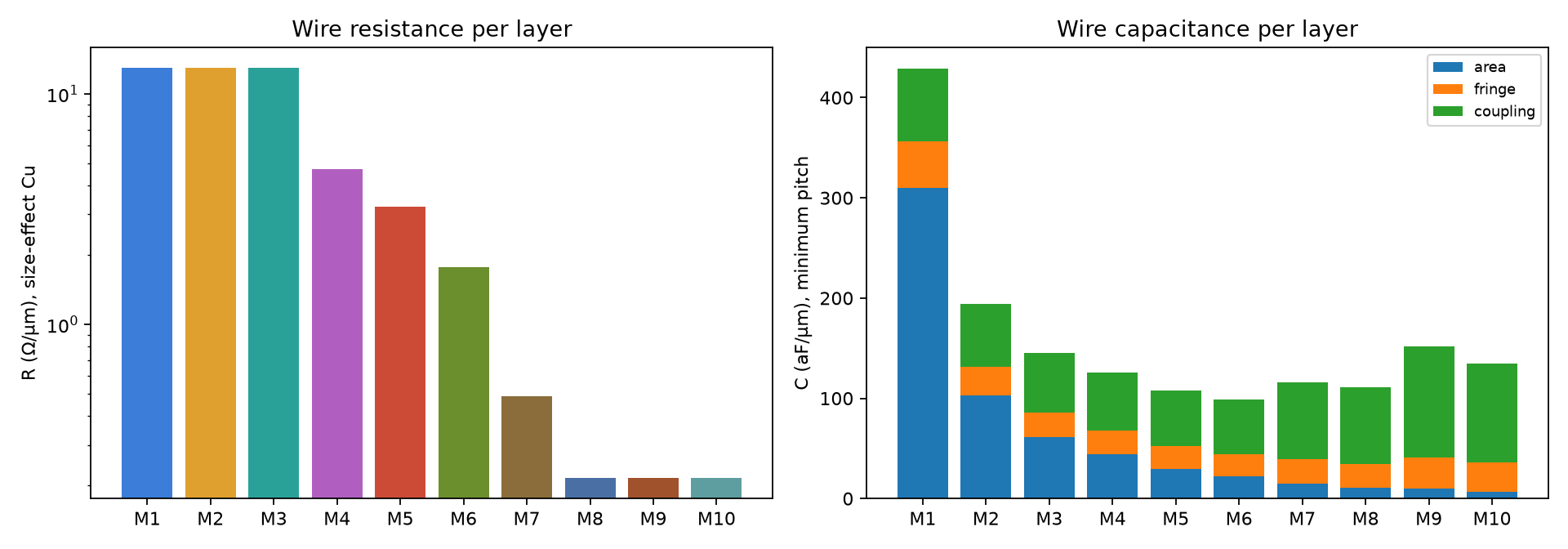
| Metal stack | 10 layers, 80 nm minimum pitch |
| Cell heights | 8 tracks (640 nm) and 12 tracks (960 nm) |
| Threshold voltages | SLVT, LVT on a flipped well; RVT, HVT on a conventional well |
| Device model | BSIM-IMG (independent multi-gate, models the back gate) |
Transistors
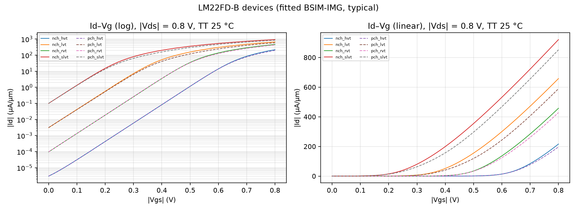
Four flavours span almost five decades of leakage. SLVT and LVT sit on a "flipped" well, so forward back-bias makes them faster; RVT and HVT sit on a conventional well, where reverse back-bias cuts their leakage.
| Device | Leakage (nA/µm) | Drive (µA/µm) |
|---|---|---|
| nMOS SLVT / LVT / RVT / HVT | 100 / 3.1 / 0.1 / 0.003 | 921 / 658 / 458 / 216 |
| pMOS SLVT / LVT / RVT / HVT | 100 / 3.1 / 0.1 / 0.003 | 852 / 589 / 428 / 197 |
Interconnect
Standard cells
- 8 libraries: four threshold flavours at two cell heights.
- 12-track: the full 130-cell set, including flip-flops, latches and clock gates.
- 8-track (dense): 115 cells. Flip-flops, clock gates and the stronger XOR cells need more wiring room than eight tracks provide, so they come from the 12-track library.
- Every cell carries separate back-gate pins (VNW, VPW), so the bias can be controlled per block.
Verified
- Every cell from its drawn layout, in all eight libraries, extracted and tested for its logic function, including the flipped-well flavours and the sequential cells simulated with the back-gate models.
- Transistors fitted to published FD-SOI data: leakage, drive, subthreshold slope, drain-induced barrier lowering, back-gate coupling and gate capacitance.
Featured analysis: back-bias
Back-bias can compensate a slow chip, an aged chip or a hot chip after manufacturing. We will characterize the libraries at several back-bias points and show how much aging and process variation a bias controller can recover, and at what cost in leakage. For timing, that means a result that depends on a run-time knob, not only on the process corner.
Built from
Published 22 nm and 28 nm FD-SOI process papers, international roadmap tables (ITRS 2011 and 2013), and the FreePDK45 research kit for the interconnect baseline.
Interactive 3D cells
Generated cells, layer by layer at true heights. Pick a cell to load it.
Drag to rotate, scroll or pinch to zoom. Heights are drawn at 2× for legibility.