LM12FF-G
12 nm FinFET, general purpose
Technology description complete; device models in progress.
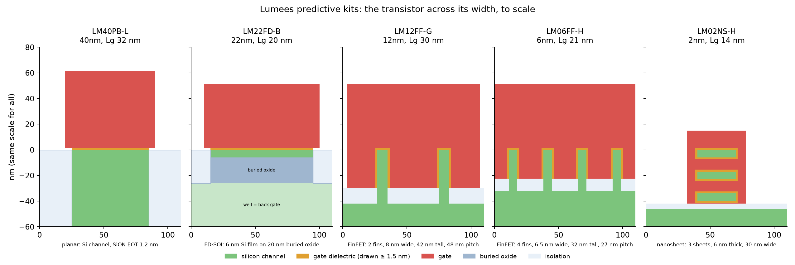
LM12FF-G is a 12/16 nm-class bulk FinFET kit, the family's first three-dimensional transistor. Current flows along tall, thin silicon fins, 42 nm tall and 8 nm wide, wrapped by the gate on three sides. That gives far better control of leakage at short gate lengths than a planar transistor, which is why FinFETs replaced planar devices below 20 nm.
Why 12/16 nm FinFET
The 12/16 nm class is the workhorse FinFET generation: mature, widely used for application processors, networking, AI accelerators and automotive compute, and the first node where many design effects tied to fins (quantized transistor width, self-heating, temperature inversion) appear.
Technology at a glance
| Supply | 0.75 V nominal |
| Contacted gate pitch | 90 nm |
| Gate length | 30–34 nm |
| Fin pitch / height / width | 48 / 42 / 8 nm |
| Equivalent oxide thickness | 0.8 nm |
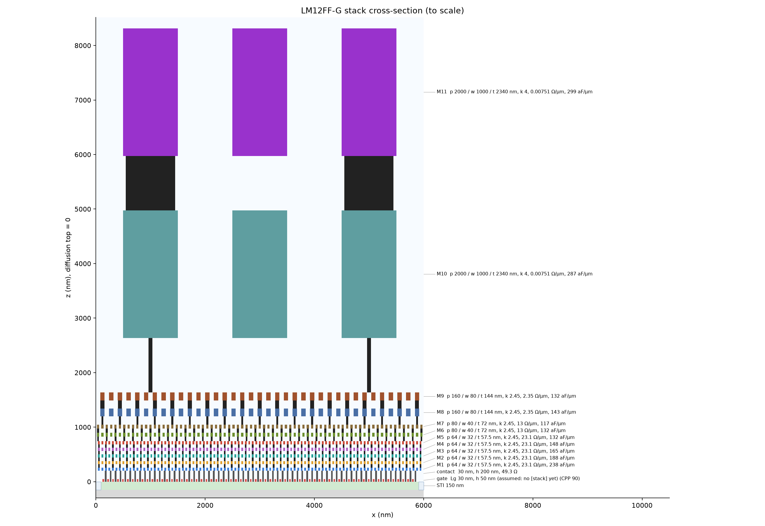
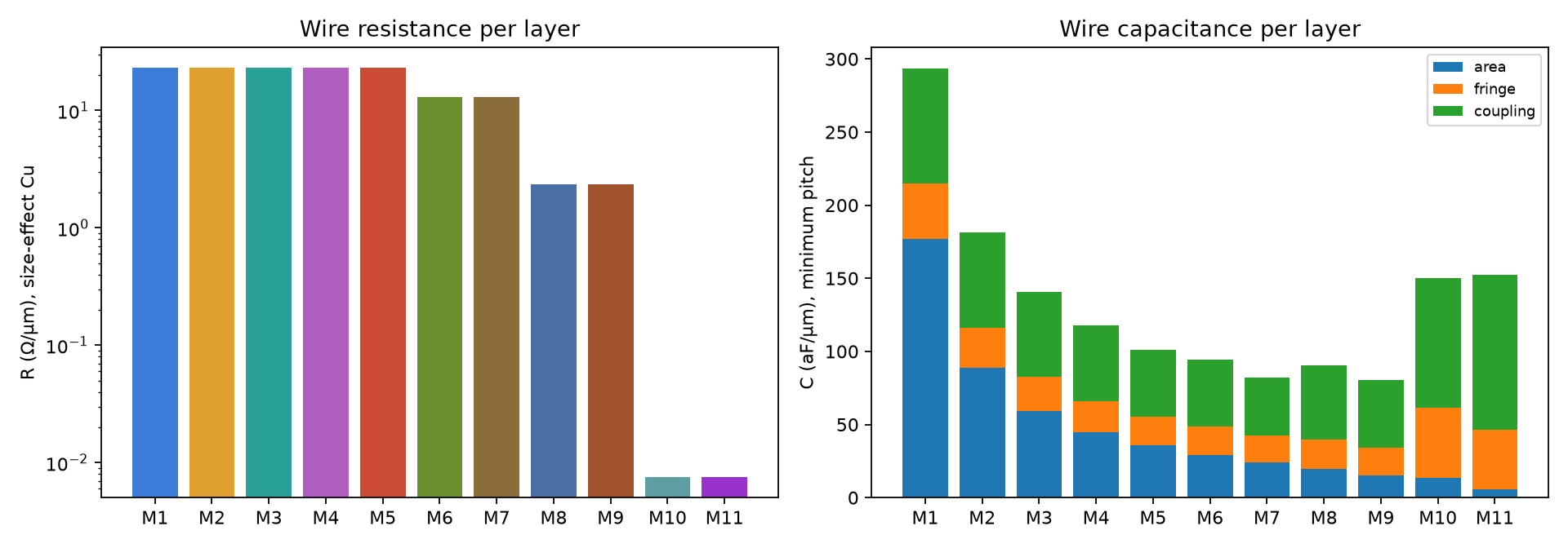
| Metal stack | 11 layers, 64 nm minimum pitch |
| Cell heights | 7.5 and 9 tracks |
| Threshold voltages | SVT, LVT, ULVT |
| Device model | BSIM-CMG |
Transistors
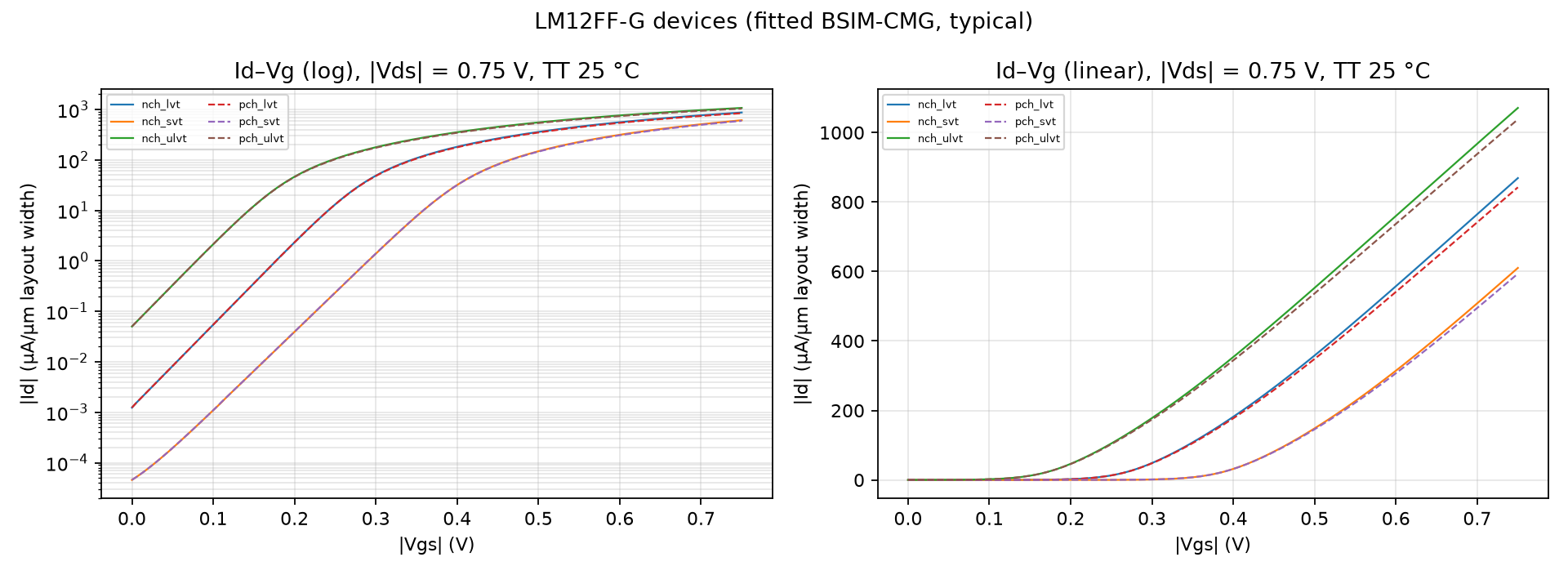
Transistor width comes in whole fins, so drive strength is quantized: a design choice our cell generator handles directly. Leakage targets are met; drive currents are being refined against published 16 nm and 14 nm data before the libraries are built.
Interconnect
Featured analysis: self-heating and temperature inversion
Fins are thermally isolated: they heat up while switching, and the heat has few paths out. At the same time, at low supply voltages FinFET circuits get faster as they get hotter (temperature inversion). Both change which operating condition is the worst case for timing. We will quantify them so that our tools pick the right corners.
Built from
Published 16 nm and 14 nm FinFET process papers, international roadmap tables (ITRS 2013), and the ASAP7 research kit's layout rules, scaled to this node.
Next
Final device fit, then standard-cell libraries at two heights and three threshold flavours, then characterization, following the same flow as LM40PB-L.