LM65PB-G
65 nm planar bulk, general purpose
Technology description and device models complete; standard cells in progress.
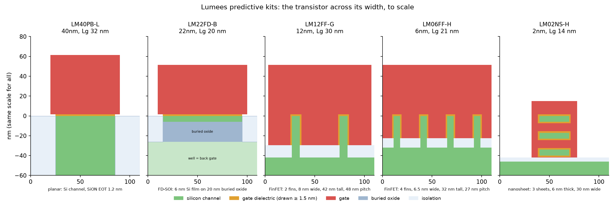
LM65PB-G is a 65 nm-class general-purpose kit: planar bulk transistors with a nitrided-oxide gate dielectric close to its thinnest practical limit, three threshold-voltage flavours, 2.5 V I/O devices and an eight-layer copper interconnect with low-k dielectric.
Why 65 nm
65 nm is one of the longest-lived generations in production: microcontrollers, wireless connectivity, image sensors, display drivers and many cost-sensitive SoCs. It sits at the end of classic scaling. The silicon-oxynitride gate oxide reached about 1.2 nm, a few atomic layers, and leakage through the gate itself became a visible part of chip power. The next generations replaced it with high-k metal gates.
Technology at a glance
| Supply | 1.1 V core (0.99–1.21 V corners), 2.5 V I/O |
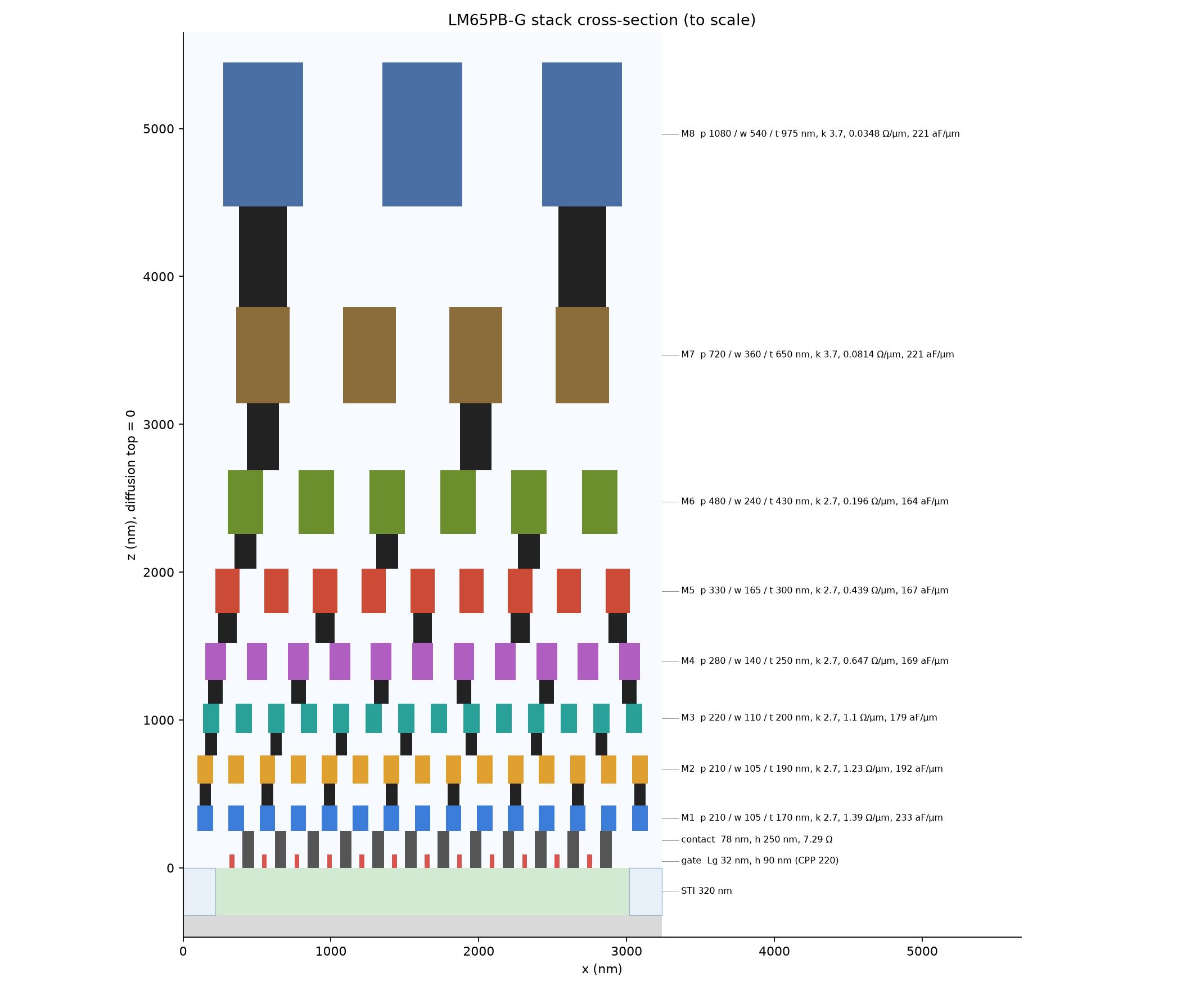
| Contacted gate pitch | 220 nm |
| Gate length | 32 nm (LVT), 38.5 nm (SVT), 45 nm (HVT) |
| Gate oxide | 1.2–1.9 nm by flavour; 5 nm for the 2.5 V devices |
| Metal stack | 8 copper layers, 210 nm first-metal pitch, low-k dielectric (k 2.7) |
| Cell heights | 9 tracks (1.89 µm) and 12 tracks (2.52 µm) |
| Threshold voltages | HVT, SVT, LVT |
| Device model | BSIM4 |
Transistors
| Device | Leakage (nA/µm) | Drive (µA/µm) |
|---|---|---|
| nMOS HVT / SVT / LVT | 0.03 / 0.5 / 9.1 | 465 / — / 563 (at 0.8 V) |
| pMOS HVT / SVT / LVT | 0.03 / 0.5 / 9.1 | 291 / — / 352 |
The HVT and LVT devices are the roadmap's low-standby-power and low-operating-power transistors for 2007; SVT lies between them.
Interconnect
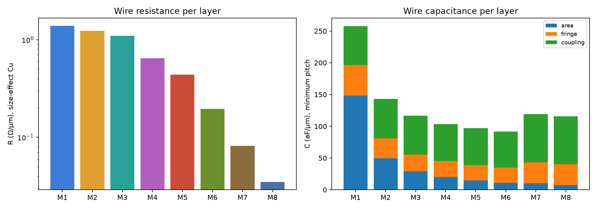
Eight copper layers, from 210 nm on the first metal to 1.08 µm on the top layer, with the pitches and thicknesses of a published 65 nm process. An earlier draft scaled our 90 nm stack by the classic generation factor of 0.7; the published stack showed that real 65 nm processes shrank gate and wire pitches much less (0.85× and 0.95×), so the draft was 17–27 % too tight. The roadmap of the time assumed even tighter wires (136–152 nm).
Featured analysis: leakage at the end of the oxide
The kit's analysis will split each cell's standby power into channel leakage, gate tunnelling and junction leakage, per flavour and temperature, and show what power gating recovers. 65 nm is the generation where gate tunnelling became a noticeable share of chip power next to channel leakage, which is why designs at this node care about standby power.
Built from
The 2007 international roadmap (devices), the 2001 roadmap (I/O devices), and a published 65 nm logic process (gate pitch and the full metal stack).
Next
The 9- and 12-track libraries, then timing characterization and the leakage analysis.