LM90PB-R
90 nm planar bulk, radiation hardened by design
Technology description (including the radiation design rules) and device models complete; hardened cells in progress.
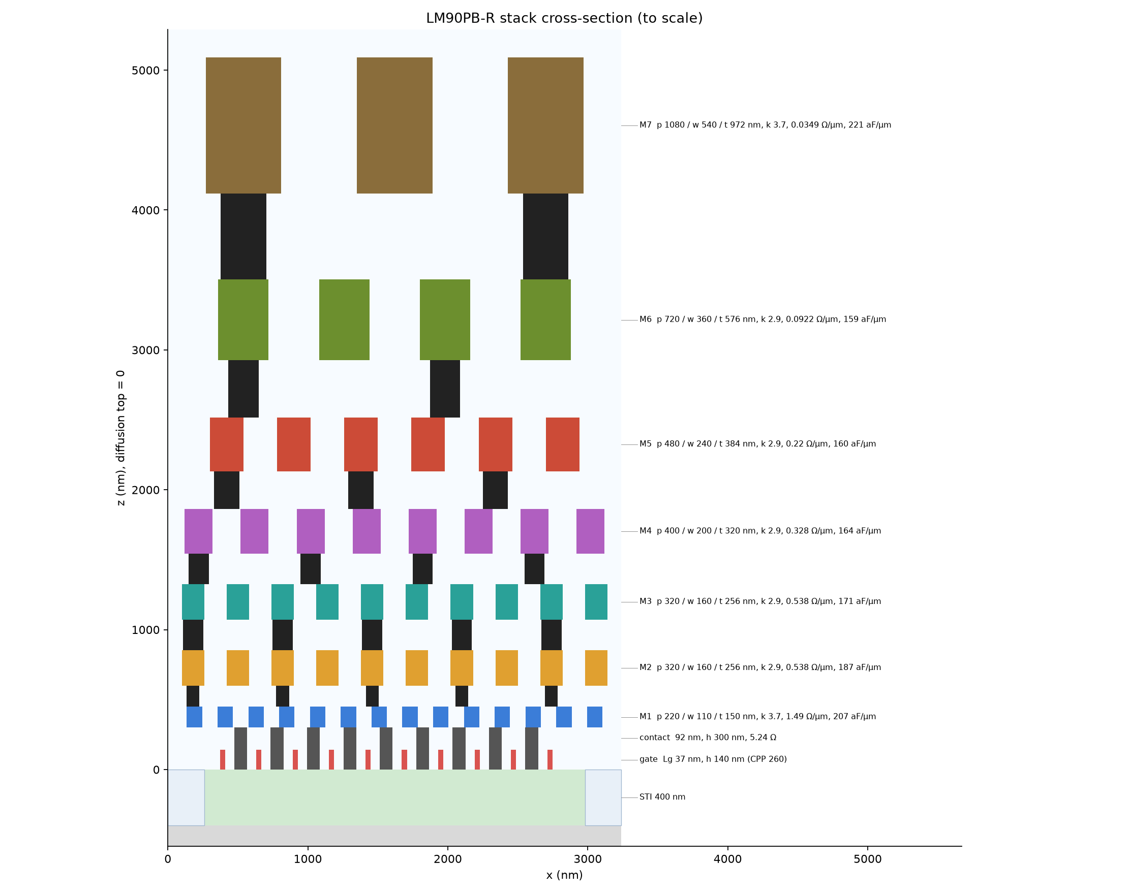
LM90PB-R is a 90 nm-class kit for space and high-reliability electronics. Its transistors and wiring are those of an ordinary 90 nm bulk process; the hardening is in the cell library. Every flip-flop and latch is a radiation-tolerant DICE cell, every cell carries its own well and substrate contacts and guard rings against latch-up, and the cells are 12 tracks tall to make room for them. The kit covers −55 to 125 °C.
Why 90 nm, and why hardened by design
Satellites, launchers and high-energy physics experiments need chips that survive radiation. Dedicated radiation-hardened processes are rare and generations behind, so most modern space ASICs are built on commercial processes and hardened by design. 90 nm is a widely used generation for this: its thin gate oxides already tolerate a high total ionizing dose, published 90 nm hardened-by-design processors have reached 1 Mrad, and the remaining risk, single particles flipping a stored bit or causing a glitch, is handled in the cells.
Technology at a glance
| Supply | 1.2 V core (1.08–1.32 V corners), 2.5 V I/O |
| Temperature range | −55 to 125 °C |
| Contacted gate pitch | 260 nm |
| Gate length | 37 nm (LVT), 53 nm (SVT), 65 nm (HVT) |
| Gate oxide | 1.2–2.1 nm by flavour; 5 nm for the 2.5 V devices |
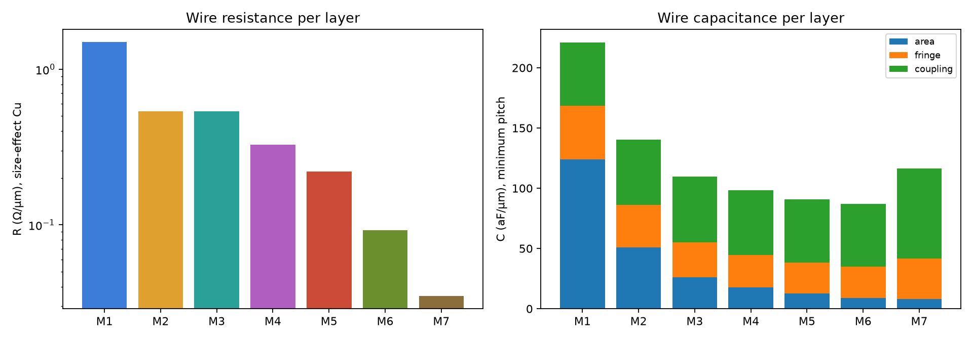
| Metal stack | 7 copper layers, 220 nm first-metal pitch, carbon-doped oxide (k 2.9) |
| Cell height | 12 tracks (2.64 µm) |
| Threshold voltages | HVT, SVT, LVT |
| Device model | BSIM4 |
Transistors
| Device | Leakage (nA/µm) | Drive (µA/µm) |
|---|---|---|
| nMOS HVT / SVT / LVT | 0.01 / 3 / 50 | 440 / 530 (at 0.9 V) / 1110 |
| pMOS HVT / SVT / LVT | 0.01 / 3 / 50 | 220 / 265 / 555 |
Radiation hardening in the cells
| Effect | What it does | How the kit handles it |
|---|---|---|
| Total ionizing dose | Slowly shifts transistors and opens leakage paths at isolation edges | Thin-oxide devices; minimum transistor widths and guard rings in place of special transistor shapes |
| Single-event latch-up | A particle triggers a parasitic thyristor that shorts the supply | N+/P+ guard rings and a tap in every cell; published data shows no latch-up up to a particle LET of 60 MeV·cm²/mg with guard rings |
| Single-event upset | A particle flips a stored bit | DICE flip-flops and latches: each bit is held on four nodes, so one strike cannot flip it |
| Single-event transient | A particle causes a short glitch in logic | Pulse widths characterized per cell, for filtering and timing margins |
Hardening has a price. Published 90 nm results put a DICE flip-flop at about twice the area and power of a standard one and 1.5 times its delay; triple modular redundancy costs four times the area and power. Our kit will measure these costs on its own cells.
Featured analysis: single-event upsets
The kit's analysis will measure the critical charge of every storage cell, standard and DICE, and the glitch width of every logic cell, by injecting the current pulse of a particle strike at each sensitive node. This gives designers upset sensitivity per cell next to the usual timing and power.
Built from
The 2003 international roadmap (devices and interconnect), a published 90 nm logic process (gate pitch and the full metal stack), and published radiation results for hardened-by-design chips on commercial 90 nm and 65 nm processes.
Next
The hardened 12-track libraries (DICE sequential cells, guard rings and taps in every cell) and the single-event analysis.