LM130PB-G
130 nm planar bulk, general purpose
Technology description and device models complete; standard cells in progress.
LM130PB-G is a 130 nm-class general-purpose kit: planar bulk transistors with a silicon-dioxide gate oxide, three threshold-voltage flavours at one 1.2 V supply, thick-oxide 3.3 V devices for I/O and analog, and a six-layer copper interconnect with fluorinated oxide between the wires. It is the oldest node in the family and its widest-margin one.
Why 130 nm
130 nm is still in volume production more than twenty years after its introduction: power management, motor control, sensors, automotive and industrial chips, and many mixed-signal designs that need 3.3 V and robust analog devices more than they need density. It is also the generation where copper wiring became the industry standard, which makes it the natural starting point for every interconnect trend in the family.
Technology at a glance
| Supply | 1.2 V core (1.08–1.32 V corners), 3.3 V I/O |
| Contacted gate pitch | 455 nm |
| Gate length | 65 nm (LVT), 90 nm (SVT, HVT) |
| Gate oxide | 1.45–2.6 nm by flavour; 7 nm for the 3.3 V devices |
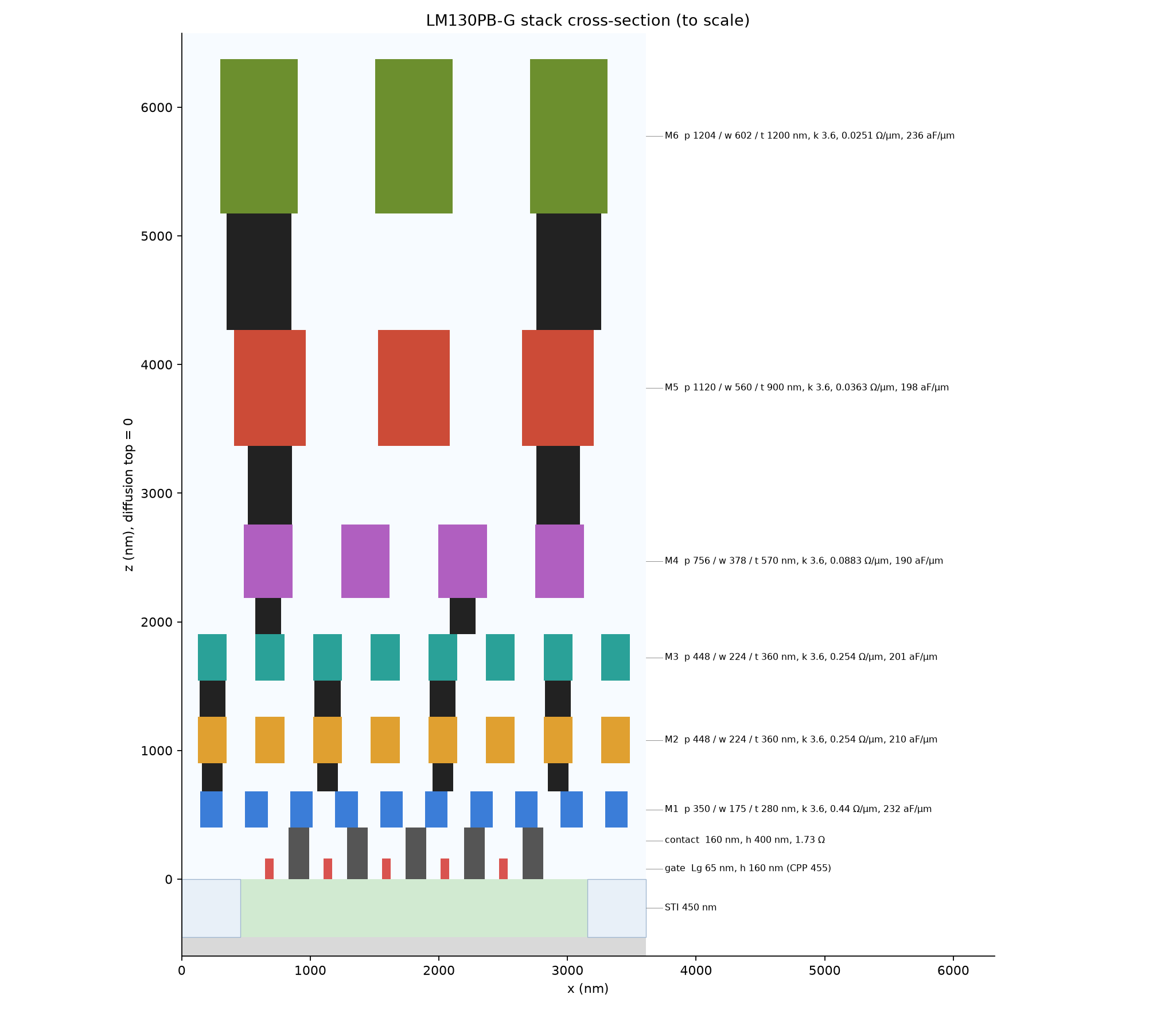
| Metal stack | 6 copper layers, 350 nm first-metal pitch, fluorinated oxide (k 3.6) |
| Cell heights | 9 tracks (3.15 µm) and 12 tracks (4.2 µm) |
| Threshold voltages | HVT, SVT, LVT |
| Device model | BSIM4 |
Transistors
The three flavours are the three logic device types of the 2001 roadmap, which in that year all ran at 1.2 V: a low-standby-power device for always-on logic, a low-operating-power device as the everyday workhorse, and a high-performance device for speed-critical paths.
| Device | Leakage (nA/µm) | Drive (µA/µm) |
|---|---|---|
| nMOS HVT / SVT / LVT | 0.001 / 0.1 / 10 | 300 / 600 / 900 |
| pMOS HVT / SVT / LVT | 0.001 / 0.1 / 10 | 147 / 294 / 441 |
Interconnect
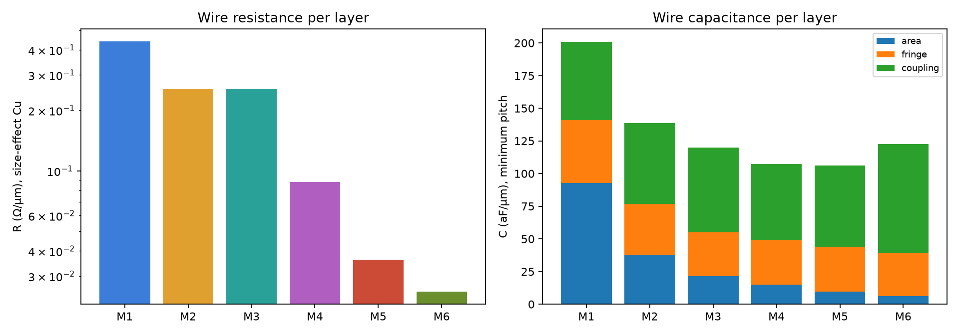
Six copper layers from a 350 nm first-metal pitch to 1.2 µm on the top layer, with the layer thicknesses of a published 130 nm process. At these widths copper is still close to its bulk resistivity: the narrowest wire has about 0.44 Ω per micrometre, more than ten times lower than at 40 nm.
Featured analysis: mixed-signal on a mature node
The kit's analysis will look at what keeps 130 nm in mixed-signal products: thick-oxide 3.3 V devices beside the 1.2 V core, and analog transistor matching against device area, from the roadmap's cited matching coefficients.
Built from
The 2001 international roadmap (devices, analog and interconnect tables) and a published 130 nm logic process (gate pitch and the full metal stack).
Next
The 3.3 V device pair, then the 9- and 12-track libraries with the same generator and checks as our 40 nm kit.